Not sure if this was uploaded before. But just a simple way of making your own pcb's.
Firstly, there are a few things you gonna have to get:
- Top of the list, a computer, DUUUR!! and a lazer printer, inkjet and all the others wont work for this tutorial.
- drill or mini drill with an assortment of bits, depending on application.
- Glossy paper or photo paper, any stationery store should have it. Try to get as thin as possible, prevents paper jams.
- A few items from a specialist electronic store, Ferric chloride (etchant) and copper clad board cut to size. Various boards available, salesman should be able to assist you with that.
- steel wool
- a clothes iron
- yours or you wife's nail polish remover
- dish washing liquid of your choice
- and lastly your pcb design
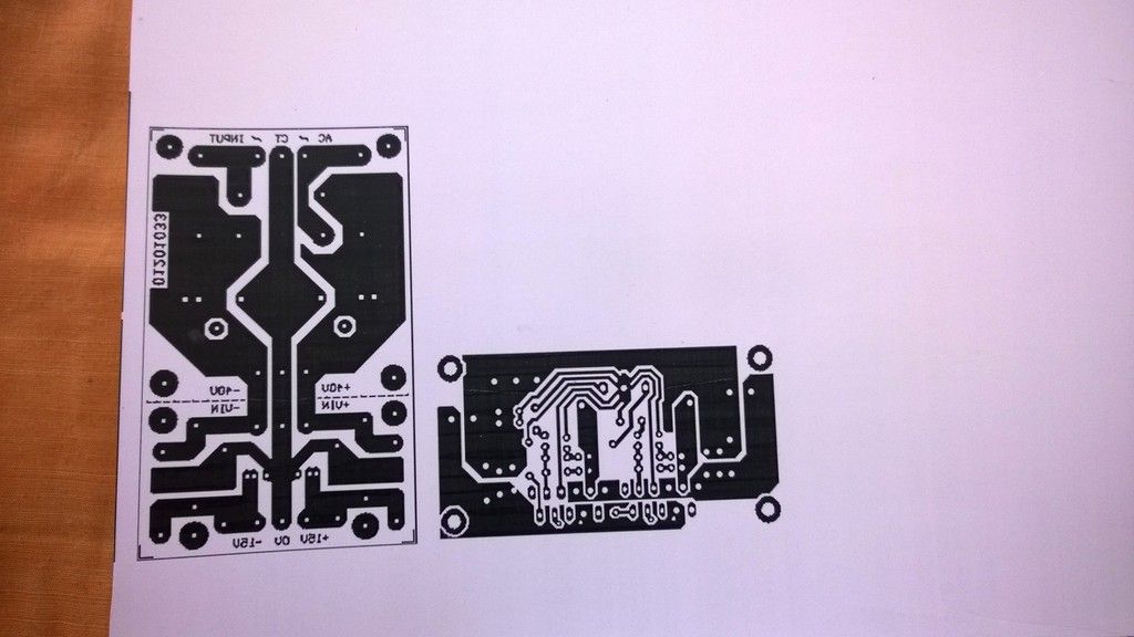
The pcb I started making earlier today was for a amplifier power supply, the actual design I got off the net (thanx to the original designer/uploader for sharing it). I resized it and cleaned it up a bit using Paint Shop Pro. Be sure to print the image on the shiny side of the paper. One thing to remember is that when you see a pcb that you would like to make, you might have to mirror the image, not flip, but mirror, or else you will be getting the layout all wrong. This can also be done with PSP. So when you looking at the image, the wording, if any, should be reversed.
So here is my image, already mirrored. See the text is in reverse!
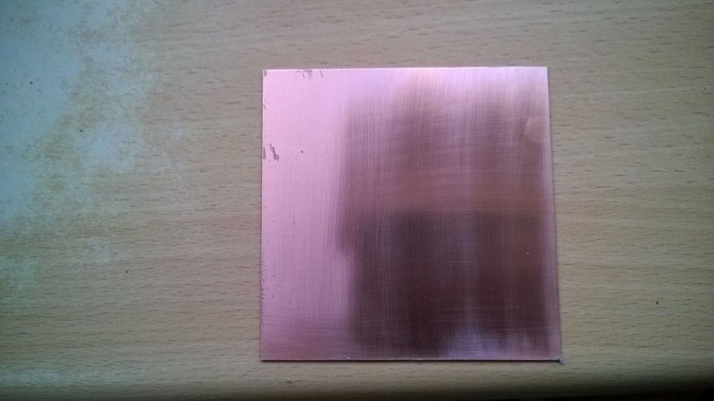
Next, we take our copper clad board, give it a nice shine with some steel wool and water, dry it off and then a good few rubs with the nail polish remover and a clean cloth. Do the nail polish remover routine a few times. make sure it's super clean. Nothing should touch the board after this.
We then take our image that we printed and lay it face down on the copper side of the copper clad board. Stick to a corner to save space. We then take our clothes iron with temp set to maximum and place it on the paper and board. This is the trial and error part. The trick is to get the thin shiny film and toner from the print on the glossy paper transferred to the copper board. Apply firm pressure for about a minute, and leave it on there for about 2 minutes. Longer is better =)
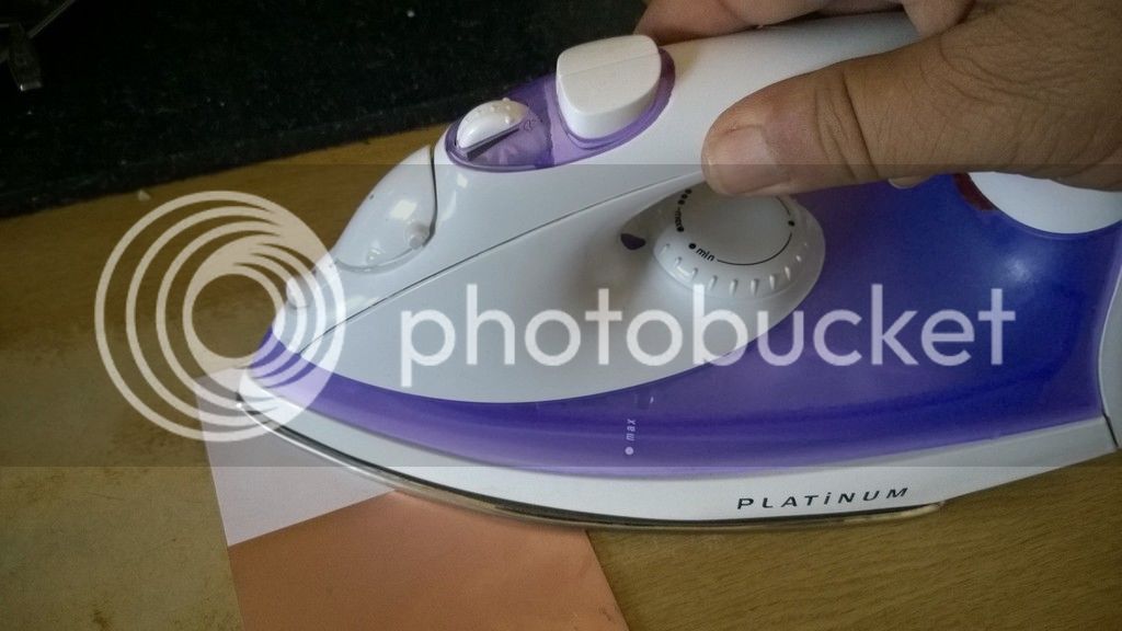
Repeat this process again.
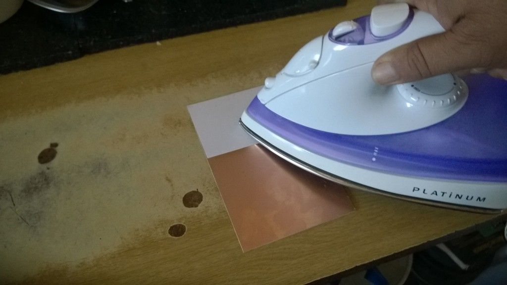
Lastly, take the tip of the iron and run it over the paper, judging where your tracks will be. These boards are quite hardy, so leaving the iron on it for a while shouldn't do any damage to it. It's important that we do not move the paper while ironing. Once this is done, take the board (careful, it's moer hot) with the paper still attached and drop it in a basin with some warm soapy liquid.
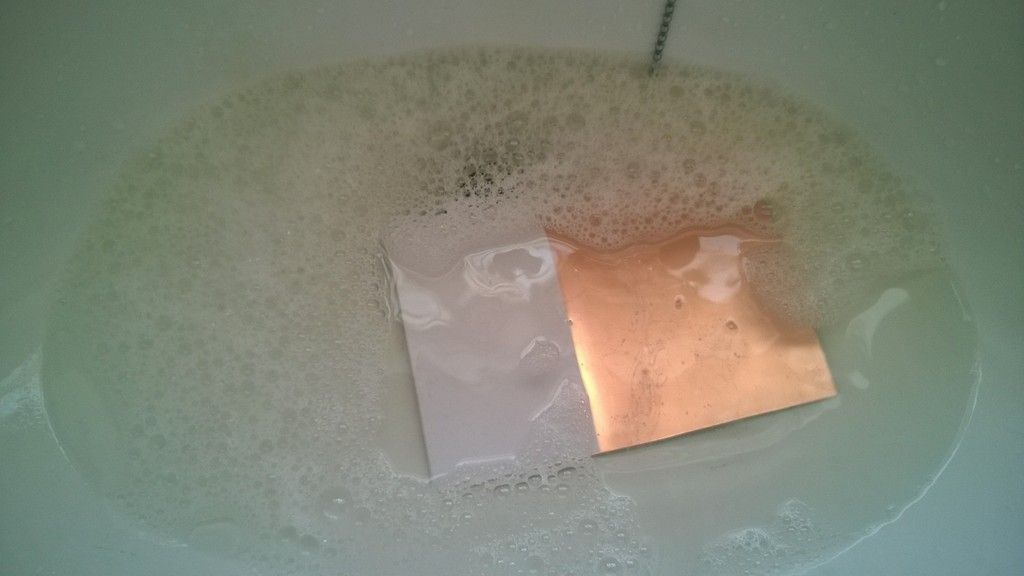
Leave it there for a few minutes until it cools down. When the board has cooled down, gently hold the paper and board with one hand and use the thumb of the other hand and rub on the paper. Be gently here, if your transfer was done properly then there shouldn't be an issue and a bit more pressure can be applied while rubbing. If any of your tracks are broken, don't worry, a ordinary black permanent marker can be used to join the tracks again, just be sure that they don't touch any of the surrounding tracks.
It should look like this
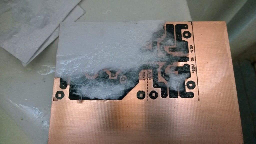
And then eventually like this
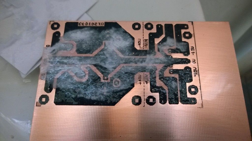
and then eventually like this
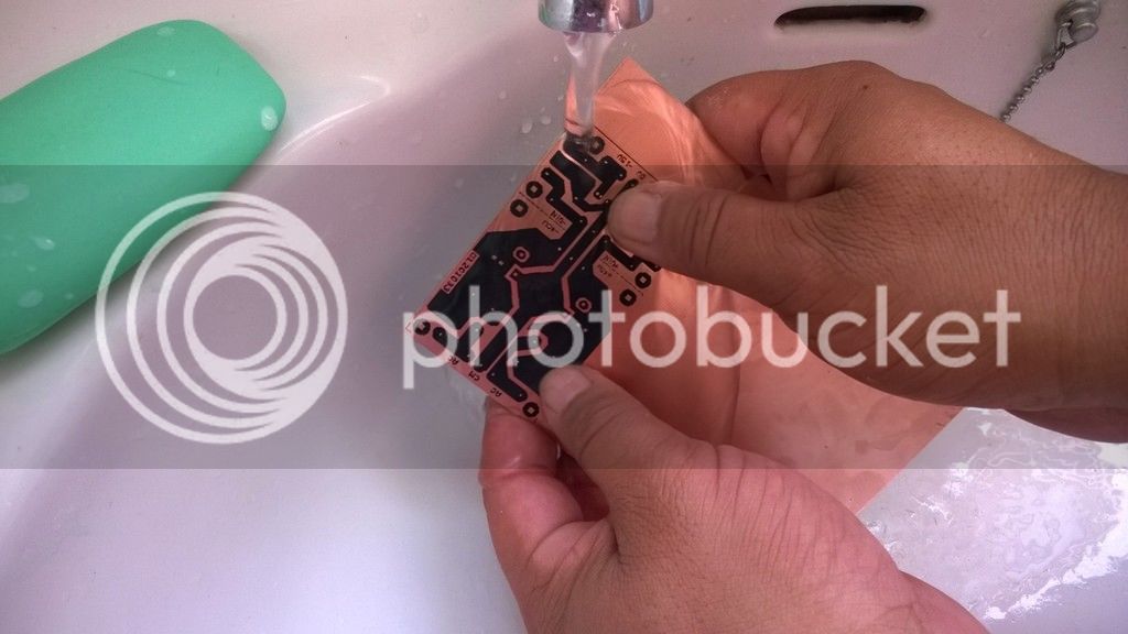
One thing, have a good look between the tracks to make sure you get all the residue off from the board. Check circles in below image. If these are not removed then the copper will remain when it gets etched. Could cause you project to blow up
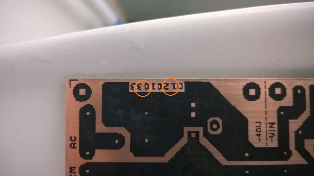
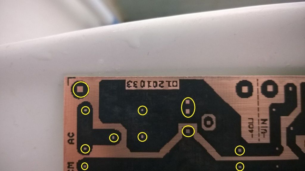
When all is done give it a good clean and then dry with a clean cloth. Before we get to the etching, the drilling can either be done now or after the etching is complete, see yellow circles. Depending if you have a little drill press etc. Once you have decided on that, we now ready to etch with the ferric chloride.
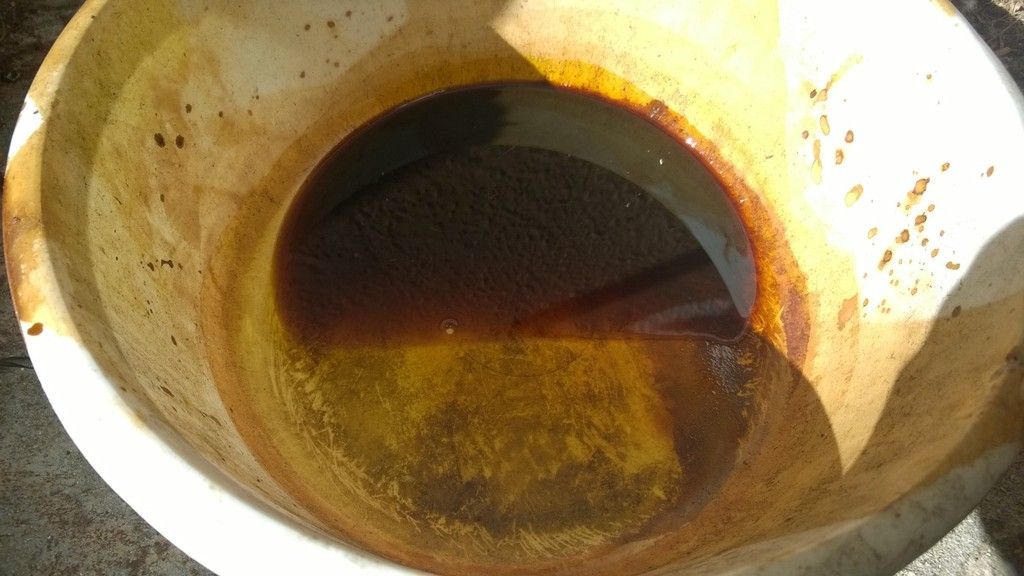
Ferric chloride! Caution, do not use this stuff in a metal container! and read the label!
Get a plastic container just large enough to hold your pcb. Place it in the container and throw in just enough acid to totally cover your pcb. Leave for 20 mins, agitating it every 5 mins or so. This whole process can be spead up buy placing your plastic container in a metal pot with hot water or just sicking it in the sun. Use you kop here.
After about 20 mins the copper board can be removed and washed with clean running water and dried.
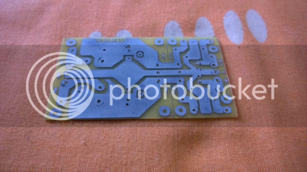
Finally, after all that is done, take some steel wool and give it a good rub until all the toner is removed from your board.
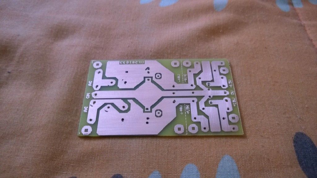
And voila!
Your board is done and ready for the components to be installed. Once the soldering and testing is done, the underside of the board can be sprayed with a clear lacquer, this should be available from the same place you bought the copper board from. With a high dpi printer and good image prep we can obtain pretty accurate results. Other methods for making ur own pcb's are available, but this is by far the easiest and cheapest method. Doing this via a company could cost hundreds of rands as minimum quantities need to be made.
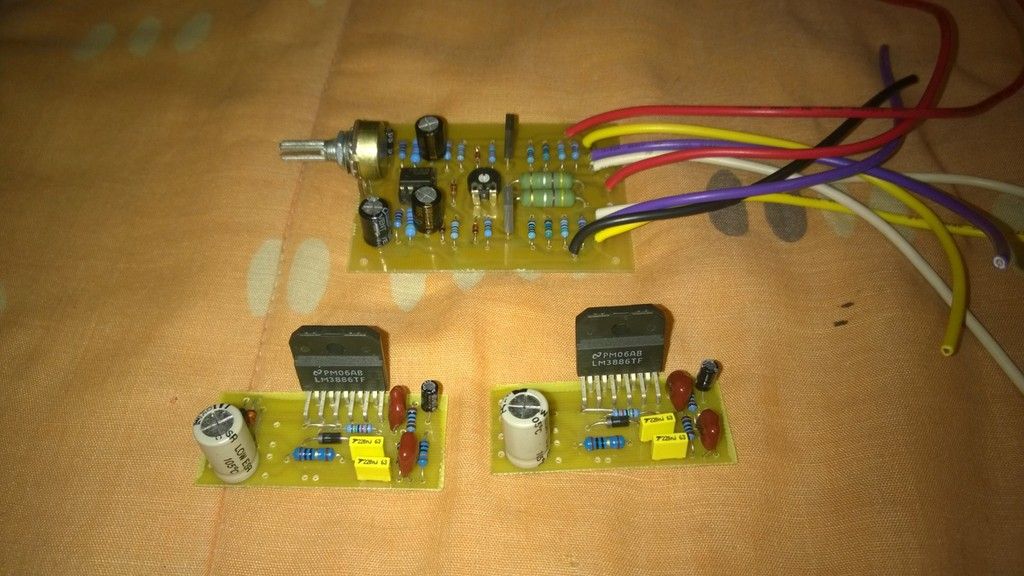
Below is some of the boards I have done in the past week using this method. Front we have 2 x 68w amp modules using the famous LM3886 IC, and the bigger one at the back is a 50w module using a 2n3055 and a MJ2955 transistor, still to be completed.
I hope this tutorial will be of help to someone. If you have any questions, pls do not ask me :BWAHAHAH:
Cheers!
Firstly, there are a few things you gonna have to get:
- Top of the list, a computer, DUUUR!! and a lazer printer, inkjet and all the others wont work for this tutorial.
- drill or mini drill with an assortment of bits, depending on application.
- Glossy paper or photo paper, any stationery store should have it. Try to get as thin as possible, prevents paper jams.
- A few items from a specialist electronic store, Ferric chloride (etchant) and copper clad board cut to size. Various boards available, salesman should be able to assist you with that.
- steel wool
- a clothes iron
- yours or you wife's nail polish remover
- dish washing liquid of your choice
- and lastly your pcb design
The pcb I started making earlier today was for a amplifier power supply, the actual design I got off the net (thanx to the original designer/uploader for sharing it). I resized it and cleaned it up a bit using Paint Shop Pro. Be sure to print the image on the shiny side of the paper. One thing to remember is that when you see a pcb that you would like to make, you might have to mirror the image, not flip, but mirror, or else you will be getting the layout all wrong. This can also be done with PSP. So when you looking at the image, the wording, if any, should be reversed.
So here is my image, already mirrored. See the text is in reverse!

Next, we take our copper clad board, give it a nice shine with some steel wool and water, dry it off and then a good few rubs with the nail polish remover and a clean cloth. Do the nail polish remover routine a few times. make sure it's super clean. Nothing should touch the board after this.

We then take our image that we printed and lay it face down on the copper side of the copper clad board. Stick to a corner to save space. We then take our clothes iron with temp set to maximum and place it on the paper and board. This is the trial and error part. The trick is to get the thin shiny film and toner from the print on the glossy paper transferred to the copper board. Apply firm pressure for about a minute, and leave it on there for about 2 minutes. Longer is better =)

Repeat this process again.

Lastly, take the tip of the iron and run it over the paper, judging where your tracks will be. These boards are quite hardy, so leaving the iron on it for a while shouldn't do any damage to it. It's important that we do not move the paper while ironing. Once this is done, take the board (careful, it's moer hot) with the paper still attached and drop it in a basin with some warm soapy liquid.

Leave it there for a few minutes until it cools down. When the board has cooled down, gently hold the paper and board with one hand and use the thumb of the other hand and rub on the paper. Be gently here, if your transfer was done properly then there shouldn't be an issue and a bit more pressure can be applied while rubbing. If any of your tracks are broken, don't worry, a ordinary black permanent marker can be used to join the tracks again, just be sure that they don't touch any of the surrounding tracks.
It should look like this

And then eventually like this

and then eventually like this

One thing, have a good look between the tracks to make sure you get all the residue off from the board. Check circles in below image. If these are not removed then the copper will remain when it gets etched. Could cause you project to blow up

When all is done give it a good clean and then dry with a clean cloth. Before we get to the etching, the drilling can either be done now or after the etching is complete, see yellow circles. Depending if you have a little drill press etc. Once you have decided on that, we now ready to etch with the ferric chloride.

Ferric chloride! Caution, do not use this stuff in a metal container! and read the label!
Get a plastic container just large enough to hold your pcb. Place it in the container and throw in just enough acid to totally cover your pcb. Leave for 20 mins, agitating it every 5 mins or so. This whole process can be spead up buy placing your plastic container in a metal pot with hot water or just sicking it in the sun. Use you kop here.

After about 20 mins the copper board can be removed and washed with clean running water and dried.

Finally, after all that is done, take some steel wool and give it a good rub until all the toner is removed from your board.

And voila!
Your board is done and ready for the components to be installed. Once the soldering and testing is done, the underside of the board can be sprayed with a clear lacquer, this should be available from the same place you bought the copper board from. With a high dpi printer and good image prep we can obtain pretty accurate results. Other methods for making ur own pcb's are available, but this is by far the easiest and cheapest method. Doing this via a company could cost hundreds of rands as minimum quantities need to be made.
Below is some of the boards I have done in the past week using this method. Front we have 2 x 68w amp modules using the famous LM3886 IC, and the bigger one at the back is a 50w module using a 2n3055 and a MJ2955 transistor, still to be completed.

I hope this tutorial will be of help to someone. If you have any questions, pls do not ask me :BWAHAHAH:
Cheers!


